JPL's Wireless Communication Reference Website

Chapter: Network Concepts and Standards Section: Data and Multimedia Systems, Infopad, Broadband CDMA Design, Monolithic RF Circuitry
Also: Analog and Digital Transmission. Section: CDMA, Rake receiver

CMOS Radio System for Wideband CDMA:
Base band Processing

Contributed by Samuel Sheng, Randy Allmon, Lapoe Lynn, Ian O'Donnell, Kevin Stone, Robert Brodersen with U.C. Berkeley Infopad Research Project

Baseband Digital Circuitry

After analog demodulation and A/D conversion, the resulting spread-spectrum digital stream needs to be decoded to recover the user bits. From the baseband block diagram for the receiver, it is evident that a massive amount of digital signal processing will be required to recover the spread-spectrum transmitted signal. In particular, the portable unit will require at least 128 MHz processing rates to perform the necessary timing recovery on the incoming 64 Mchip/sec signal, and multiple receivers to track and resolve multipath arrivals. Clearly, the power needed to drive these functions can easily be prohibitive for portable operation. The total power consumption must be minimized, while maintaining the required throughput of the overall system. However, since the processing is bounded by real-time constraints (with Tchip = 16 nsec), once the throughput performance is met there is no advantage is making computation any faster, opening up a major degree of freedom to the designer. In the analysis below, we will focus on the design and power minimization of the receiver baseband DSP, given its extreme power requirements and complexity.


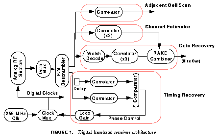
FIGURE: Digital baseband receiver architecture

Power Consumption

Techniques have been developed which reduce power consumption in CMOS digital circuits while maintaining computational throughput, by trading off area for power savings. The key source of power dissipation in digital CMOS circuits is the switching current, which is summarized in the following equation:

P total = (CL · Vdd2·f clk)

CL is the effective loading capacitance, fclk is the clock frequency, and Vdd is the supply voltage. Thus, minimizing CL, Vdd and fclk, while retaining the required functionality becomes paramount. The reduction of Vdd is the key to low-power operation; however, a speed penalty is incurred by this, and must be compensated by architectural modifications in the system, by incorporating parallelism or pipelining. To optimize power, the supply voltage can be used as a design parameter. Three supply voltages are used: 1.5V, 3.3V, and 5V, with the multiple supply voltages being efficiently generated from a single battery using off-chip DC-DC converter circuitry. These voltages were chosen to match the supply voltages used by other chips in the mobile terminal (3.3V and 5V), plus a single "low-power" supply at 1.5V. The 1.5V figure has been shown to be the optimal supply voltage under certain assumptions. Likewise, level shifting buffers are used on- chip to interface between blocks at different supply voltages. Another technique used to optimize power was the choice of number representation. Since the sign of the data is constantly being toggled due to the multiplication with the Walsh and PN sequences, it was found that a sign-magnitude number representation will consume approximately 30% less power than a 2's complement number representation for this application.

Matched Filter Correlator

The critical block in the receiver is the matched-filter correlator. A total of 9 complex-valued (in-phase and quadrature) correlators will be needed to implement the required functionality. To simplify matters, the input data mux decimates the 128 MHz I/Q streams down into two parallel 64 MHz streams for processing. Due to the nature of the delay-locked loop, this can readily be done, since one stream will be fed into the timing recovery loop, and the other stream will be fed into the data recovery and RAKE estimator blocks. Each complex correlator consists of a pair of identical datapaths, one to correlate I and one for Q. The input is a 4-bit sign-magnitude value, clocked in at 64 MHz. Using the sign bit for control, the 3-bit magnitude is directed into a positive or negative accumulator; each accumulator is 9 bits wide to account for the required dynamic range for 64 samples during correlation. After the correlation is completed, the contents of the negative accumulator are subtracted from the positive accumulator resulting in a significant power savings, as the subtraction only needs to be done at a 1 MHz rate.


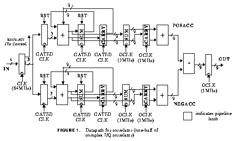
FIGURE: Data path for correlator


Lastly, to be able to reduce the supply voltage down to 1.5V for the correlator datapaths, minimizing the critical path in the accumulator itself is mandatory. To achieve this, a carry- save adder architecture is employed; it effectively pipelines the adder at the per-bit level, reducing the critical path down to the delay through a single half-adder and a register. Each correlator thus can achieve the full 64 MHz throughput, running at a supply voltage of 1.5V, while only consuming 1.5 mW of power for each complex-valued correlator. To contrast, had a ripple-carry adder been employed in the accumulator, it would have needed to run at a 3.3V supply to meet the critical path (carry ripple through 9 bits), and power consumption per complex correlator would have increased almost fourfold, to 5 mW each.

Due to the fact that the clock generator needs to be able to adjust its phase very accurately (since it is being driven by the delay locked loop), it must run at 256 MHz, and consumes a significant fraction of the power since a supply voltage of 5V is needed. Otherwise, by minimizing the power consumed in the correlators, the total power consumption of the digital baseband receiver processing has been minimized to 27 mW, despite its extremely high operating frequencies.


JPL's Wireless Communication Reference Website © Samuel Sheng, Randy Allmon, Lapoe Lynn, Ian O'Donnell, Kevin Stone, Robert Brodersen and 1993, 1995.