JPL's Wireless Communication Reference WebsiteChapter:
Network Concepts and Standards
Section: Data and Multimedia Systems, Infopad,
Broadband CDMA Design,
Monolithic RF Circuitry
|
For several reasons, direct sequence spread-spectrum, or code-division multiple access, becomes attractive for use in the downlink. The Infopad CDMA system itself is a wideband extension of the U.S. IS-95 digital cellular CDMA standard, which utilizes a transmitted synchronization tone for timing recovery and Walsh orthogonal codes to multiplex users. A basic raw user data rate of 2 Mbps is assumed to allow a margin for channel error correction as well as the ability to explore various compression algorithms. The raw data is then modulated into a 1 Mbaud DQPSK symbol stream. In determining the cell size of 5 meters, a typical office environment consisting of soft-partition cubicles is assumed, with each cell typically containing 12-16 active users. Of those 16 users, it is assumed that approximately half are demanding the full 1 Mbaud data rate for video use, while the remainder are utilizing 128 kbaud (256 kbps) each for lower data rate applications such as voice or text/graphics.
First, the greatest power consumption in existing analog cellular phones lies in the power consumed by the transmitter. Since the transmit power must be scaled down as the cell radius is reduced, power consumed in the portable to drive the antenna drops correspondingly. Whereas existing cellular systems utilize 1 watt transmit power for RF links in 5 mile cells, a picocellular system with 5 meter cells only requires 0.1 to 1 milliwatt to maintain the link. The impact of this is tremendous: the traditional RF power amplifier is not needed, and transmit power becomes a small fraction of the overall system power consumption in a microcell or picocell environment.
Hence, power minimization of the remaining RF components becomes critical. Shown in figure 4 is the block diagram of conventional superheterodyne RF transceiver designed for picocell operation in the 902-928 MHz radio band. Implemented using commercially available components, the power consumption for each active element in the transceiver is indicated. Even without the transmit power amplifier, the total consumption is impressive: 1W overall, with 750 mW being consumed in the receiver. Furthermore, the component count is astronomical: over 200 passive and active devices are needed to implement the design, after taking into account external bypass, filter, and bias elements. To minimize both the power and component count, the development of highly integrated analog technologies is thus dictated. The greatest gains are to be had from optimizing the receiver circuitry, given the complex chain of amplifiers, mixers, filters, oscillators, and A/D converters required to implement it.
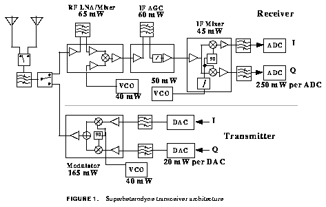
FIGURE: Superheterodyne transceiver architecture
Thus, we will focus on the design and implementation of a single-chip, highly integrated receiver capable of operating in the 1 GHz frequency band and supporting a 64 Mchip/sec direct sequence spread spectrum signal. To facilitate high integration levels, silicon CMOS is employed exclusively in the design.
As a demonstration, the RF amplifier design been fabricated and tested in a 1.2 micron technology. The design is a two-stage trans-conductance- tran-sresistance cascade, with the tran-sresistance stage consisting of the tightly coupled feedback loop formed by NMOS' M2-M3. The presence of this feedback loop ensures that the circuit has no high-impedance nodes, thus achieving its broadband performance. Since the trans-conductance stage has gain gm1, the overall gain of the circuit is thus gm1/gm3, which is can be shown to be process and temperature independent. The output buffers shown are needed to drive an off-chip filter stage, and are designed to be matched to 50W.
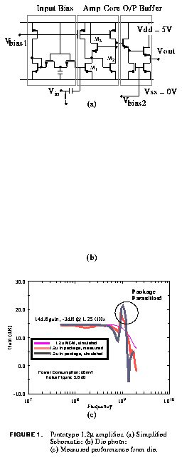
FIGURE: Prototype 1.2m amplifier. (a) Simplified Schematic; (c)
performance;
The circuit was originally designed for use in a low- parasitic multichip module; however, for testing it became necessary to package the device in a 44-pin leadless chip carrier. The sharp peaking near the rolloff corner is due to the extra parasitics introduced by the package. The SPICE simulation for the amplifier with the package can be seen to fit quite well to measured values, and the SPICE simulation of the device in a multichip module is also shown. A version of this amplifier correcting for the package parasitics has been designed, and will be fabricated shortly as part of the integrated receiver circuit.
In any case, the system design must take this phenomenon into account, since it is impossible to achieve zero offset. First, two sampling switches are employed to recover both the in-phase and quadrature signals; thus, this frequency offset can be viewed as a slow rotation of the constellation in symbol space. Also, it is clear that the offset will be significantly smaller than the user symbol rate (1 MHz) given a typical frequency accuracy of 20 to 100 parts/million for crystal-based references. Thus, by employing an incoherent DQPSK digital modulation, the effects of the frequency offset can be nullified without the use of a carrier phase-locked recovery loop. Although a 3 dB SNR penalty is incurred by the incoherency, there are alternative strategies to recover this 3 dB that are far less expensive than carrier recovery, such as employing diversity antennas or error correction coding.
In order to meet the performance requirements for the spread-spectrum downlink, a sampling switch capable of handling a 1 GHz modulated signal and running at 128 MHz (twice the chipping rate) has been developed. First, to minimize the effects of switching noise and charge injection, a differential bottom- plate sampling topology is employed. Second, the sampling capacitors must be able to track the 1 GHz modulated signal in order to sample the signal. Hence, the switches M1a,b and M2 must be carefully sized to ensure that the lowpass cutoff (formed by the on-resistance of the switches and the sampling capacitor) is well in excess of 1 GHz; otherwise, the incoming RF signal will be disastrously attenuated.
Furthermore, to achieve the 128 MHz switching performance, an extremely fast opamp is needed; in order to minimize the amount of static current in the opamp (and hence power), a unity-gain architecture is employed, in which the sampling capacitor itself is used in the opamp feedback by opening switches M1a,b and closing switches M3a,b. This is has been shown to maximize the feedback factor for the closed-loop opamp. Since settling time is proportional to 1/(Gmf), where f is the feedback factor and Gmis the opamp transconductance gain, for a fixed settling time, increasing f translates to a decrease in the gain Gm, and correspondingly resulting in a minimum power solution to achieve the necessary settling time.
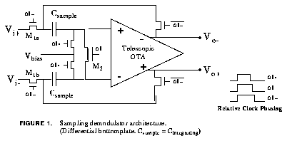
FIGURE: Sampling demodulator architecture. (Differential bottomplate,
Csample = Cintegrating)
Intuitively, beyond a certain number of bits resolution, there should be no improvement in system performance by increasing the resolution further. Essentially, at this point, both the dynamic range and quantization noise requirements have been met. To determine this, the simulation results for BER vs. number of users for varying A/D converter resolutions are shown in figure 8 for a worst-case (extreme fade) channel. Beyond 4 bits, no improvement in the BER curve is seen. The result is surprising, in that the required number of bits is far lower than expected. However, this makes sense: quantization noise itself is an additive phenomenon, the matched filter correlators will serve to reject this noise as well, effectively providing more bits of resolution at the output of the correlators.
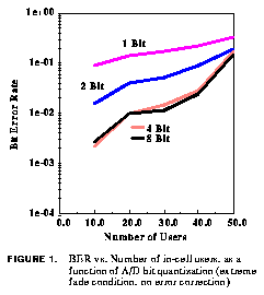
FIGURE: BER vs. Number of in-cell users, as a function of A/D bit quantization
(extreme
fade condition, no error correction)
Therefore, a 128 Msample/sec A/D converter has been designed for integration with the analog receiver and the digital baseband circuitry. The need for only four bits of resolution, along with the high sampling rate imply a flash architecture for the A/D converter. However, the need for a low power design leans towards a pipelined architecture. This is mainly due to the fact that the switched-capacitor sample-and-hold circuit already designed for the sampling demodulation can be easily be modified to act as a natural interstage gain amplifier for a 1-bit per stage pipeline. Unfortunately, the 128 MHz sampling rate makes a full pipeline implementation prohibitive, given the extreme critical path constraints. However, the final stage of a pipeline does not have the same constraints as previous stages. Therefore, a hybrid 1bit-3bit pipeline has been implemented in which a 3bit flash converter is preceded by an interstage latch and a 1 bit converter to determine the most significant bit. In this manner, a traditional 4 bit flash comparator is reduced in complexity from 15 comparators to 8. Its comparison time after the input stabilizes is under 3 nsec. More importantly, the complete 1-bit/3-bit pipeline consumes only 20 mW of power to achieve the desired goal of 4 bit, 256 MHz conversion.
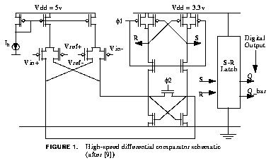
FIGURE: High-speed differential comparator schematic
The final architecture for the analog receiver is shown in figure 10, and is going into fabrication soon. As compared to the 750 mW superheterodyne receiver, it consumes only 60 mW of power, gained primarily through the use of a switching demodulator to minimize the hardware. Furthermore, the fact that no off-chip loads need to be driven after the first amplifier stage also minimizes the amount of power expended in high-frequency board drivers. Lastly, the use of spread-spectrum minimizes the quantization accuracy required in the A/D converter, which permits a low-power solution to the analog-digital interface circuitry in spite of the extremely high speeds required
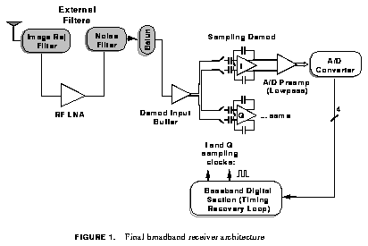
FIGURE: Final broadband receiver architecture


![]()